

3D IC異質整合複雜度高
由於3D IC的研發工作是一件龐大的整合工作,初期研發不是一間公司所能負擔的起,加上其異質整合的特性,雖然號稱可以不必使用最前衛的CMOS技術,不過整合複雜度其實會超過SoC設計。目前,從亞洲到歐洲及美國都成立了一些研發聯盟來堆動 3D IC的研發工作。這些聯盟就是希望異業結合,來創造一個虛擬的IDM,所以不同於一般的 IDM廠,他們整合製程、材料、儀器、測試封裝等上下游之產業鏈,嘗試以分工合作的角色來垂直整合3D IC的研發工作,基於一個共同的測試平台或製程,做到相互扶持,利益分享、知識分享與風險分擔。各個團隊所在地區不同,組合狀況也不同。基本上有的以製程為主,其整合晶圓代工廠、專業封裝廠與材料及設備商,有的以標準制定為準,當然也有以學研單位為主。以下為目前收集到的一些世界上推動3D IC 的單位或聯盟。我們分為二期幫大家介紹。
Pidea
這是一個歐盟Eureka Cluster計畫下的組織。這個計畫著重於高密度的連線與封裝技術[1]。雖然這個計畫時程僅有2002~2005 年,但是,當時即點出了高密度連線技術下的可能的應用方向。當時也已經希望用記憶體堆疊來證明晶圓級封裝(WLP)的技術能力[2]。
應用方向包括:
其會員組成如圖一所示。
《圖一 Pidea 會員示意圖》 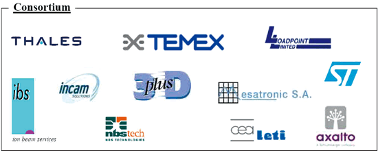 |
EMC 3D 論壇(EMC 3D)
EMC-3D(Semiconductor 3D Equipment and Materials Consortium)成立於2006年9月,這是目前所知較大的一個3D-IC論壇,參與的廠商偏向設備與材料領域,其相關公司如表二所示。EMC-3D目標為2009年能達到每片晶圓擁有成本(Cost of Ownership)低於美金200美元以下,EMC-3D發展的技術主要希望可以用DRIE或者雷射方式達到via介於5um~30um之間,並使用12吋晶圓。
該組織成立後的三年的目標就訂為:
Year |
Goal |
Year 1 |
Demonstrate integration (or stackability) of via-first TSV technology on 200mm wafers with members’ equipment and process technologies with CoO≈400-500$ / wafer. |
Year 2 |
Demonstrate integration and reliability of TSV technology(via-first or via-last depending upon technology trends) on 200mm wafers with members’ equipment and process technologies with CoO ≤300$ per wafer. |
Year 3 |
Demonstrate seamless integration and reliability of TSV technology (via-first or via-last depending upon technology trends)on 300mm wafers with members process and equipment technologies with CoO of < 200$ / wafer. |
到了2008 年EMC3D至少做到了:
其中Barrier Layer由於銅本身擴散係數高,以及在矽基材中形成深層能階,便元件電性劣化。再者,銅對介電層的附著性差,因此需要一層擴散障礙層作為銅與介電層之間的緩衝層。現今研究中的銅擴散障礙層中有:TiN、WN、TiWN以及TaN等等。這些材料具有高溫熱穩定性及良好的導電性,在這些材料中,鉭為主的材料具有較佳的抗銅穿透能力。鉭本身不會和銅形成化合物,因此Cu/Ta/Si的結構在高溫下仍非常穩定。對氮化鉭來說,其晶粒縮小,氮在氮化鉭中的含量增加,可以有效抑制銅原子的快速擴散。
Catalog |
Company |
Website |
Note |
Equipment |
Semitool |
Plating, Thinning (Wet-etch based) |
|
Alcatel AAMS
|
Via Etch, Dicing (Dry-etch based) |
||
XSiL
|
Via Drill, dicing (Laser-drill based) |
||
EVG
|
Stacking, Alignment, Resist process |
||
Isonics
|
Sequential Wafer Thinning |
||
|
Datacon
|
Die-to-Wafer pick and place, Die Bonding |
|
Materials |
Rohm and Haas PFT |
Plating chemicals |
|
AZ |
Photoresists |
||
Enthone (Cookson Electronics)
|
Plating chemicals |
||
Brewer Science |
Adhesives |
||
R&D Partners |
SAIT (Samsung Institute of Technology) |
Sensors/MEMS/Chip stacking |
|
Fraunhofer IZM |
Sensors/MEMS/Chip Stacking |
||
KAIST (Korea Advanced Institute of Science and Technology) |
Chip stacking |
||
TAMU (TexasA&MUniversity)
|
Electrochemical Studies |
||
CEA-Leti
|
|
Sensors/MEMS/Chip Stacking |
|
NXP
|
Sensors/MEMS/Chip Stacking |


3D 全矽製程模組論壇(3D All Silicon System Module Consortium;3DASSM)
此聯盟由喬治亞理工學院的微系統封裝研究中心(Microsystems Packaging Research Center)與位於德國柏林的IZM-Fraunhofe及南韓的KAIST共同成立。從這個組織的名稱就知道這是一個希望以矽製程來完成所有3D IC「矽統」設計工作的團隊。
從圖二來看,Die與Die之間的連線並不全然靠TSV,從圖上得知,Die2有挖TSV,Die3則沒有,所以這兩個Die可能是以Flip Chip且以面對面的方式堆疊。Die1與 Die2則透過下層的矽基底用TSV相連,最下層則以傳統的Solder Bump 與外界相接。
《圖二 3D ASSM 聯盟的3D IC(2008)[4]》 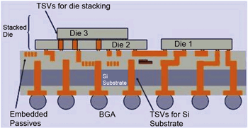 |
2008年主要工作內容如下,大致上分為六大類[4][5]:
3D All Silicon System Module Design
著重在全矽製程的3D IC 模組,這部分的目標包含了如下的一些技術:
Si Substrate with Multilayer Wiring and Shielded TSV
希望以矽基底提供多層的繞線可能與具有防護功能的 TSV,這部分的目標包含了如下的一些技術:
Low Cost TSV
低成本的TSV這部分的目標包含了如下的一些技術:
Thin Film Active and Passive Components
薄膜式的主動或被動元件,這部分的目標包含了如下的一些技術:
IC to Si Substrate-Board Interconnections and Reliability
晶粒到基底電路板的連接技術與可靠性,這部分的目標包含了如下的一些技術:
Advanced Thermal Solutions:
前瞻的熱處理能力,這部分的目標包含了如下的一些技術:
圖三則是3D ASSM的另一個3D IC 的夢想,這個3D IC比圖二多了很多技術需求。首先,我們發現有不同尺寸大小的TSV,也就是有大的由最上貫穿Silicon Core到最下層,也有尺寸小的TSV,它用以貫穿幾個不同的Die,這些Die又被包圍在一個Silicon Core中。圖四為3D ASSM 的發展重點。圖五是3D ASSM認為3D IC/TSV不同的應用層次,左圖為兩個晶粒單純利用TSV垂直相連,中間TSV與Interposer結合的晶粒堆疊,右圖完整的一個晶圓片的模組。表三則是3D ASSM針對WLP所用到的Interposer 所定的目標規格。
《圖三 3D ASSM 聯盟的3D IC理念》 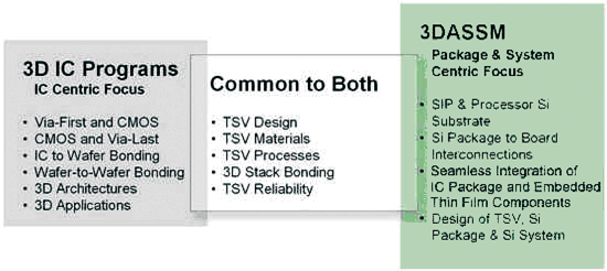 |
《圖四 3D ASSM 聯盟的發展重點(2009)》 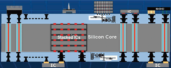 |
《圖五 3D ASSM聯盟的3D IC應用層次(2009)》 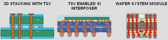 |
Si Core Thickness |
150-200um |
Substrate Lines/Space |
1-5u for research, 10u for phase 1 demonstrator |
Build-up Layer Via/Pad Size |
10-25um Vias, Via-pad registration <10um |
\# of build-up dielectric layers |
2 on each side |
Total metal layers |
6 |
Dielectric Material |
Low modulus, Low CTE thermosetting |
Dielectric Layer Thickness |
10um per layer (dry film) |
Metal Thickness |
3-5um per layer |
Cost |
Comparable or less than organic substrate benchmark |
Reliability |
JEDEC standard, MSL pre-conditioning (Level 2-3), 3x Solder reflow at 260OC, 1000 cycle -40 to 125 TC, HAST 121 C, 85%RH, 96 hours |
Conductor loss |
<0.1dB per mm |
Dielectric loss |
< 0.005 @1GHz |
Tolerance |
+/-% on lines/spaces, thickness |
3D IC Alliance
這個聯盟由兩家主要的3D-IC設備商所創立:Tezzaron與Ziptronix。目前,較為重要的成就是公佈了一個針對記憶體的3D-Memory規格IMIS(Intimate Memory Interconnect Standard)。
這個標準是由3D-IC聯盟發起的記憶體互連標準(Intimate Memory Interconnect Standard;IMIS),用來制定3-D堆疊記憶體晶片的官方標準。記憶體包含了SDR DRAM、DDR DRAM和DDR Flash、QTR DRAM、NBT SRAM、DTR SRAM、QTR SRAM和Dual Port。這個標準到了2008年6月1日才有第一個版本制定出來[6]。
Intimate有點是接觸皮膚的意思,亦即在記憶體表層定義一個高頻寬的垂直匯流排,以便讓上層的主控制Host IC 可以與其相連。記憶體 IC與主控制IC雖然是分別製造,但是,記憶體IC看來就像是主控制IC的嵌入式記憶體。所以不需要準備特別的chip-to-cip I/O,即使是ESD元件也可以省了[7]。IMIS所定義的頻寬高達1024bit。標準內定義一個 I/O Port(Pin Grid),Port的高度為450um(19 pin),寬度為2000um(80 pin),如圖六所示。
每一個Pin就是一個Cell,每個Cell的大小為25um×25um(註),在這個面積裡面,每一個Pin的實際面積大小是15um×15um。表四為IMIS定義之Pin,因為橫向的大小有2000um,共有80 Pin,所以這個表格只是全部表格的1/8。目前已經有該聯盟的發起成員Tezzaron半導體和Ziptronix並已開始製造採用IMIS埠的記憶體晶片。(待續)
《圖六 IMIS Port Layout》 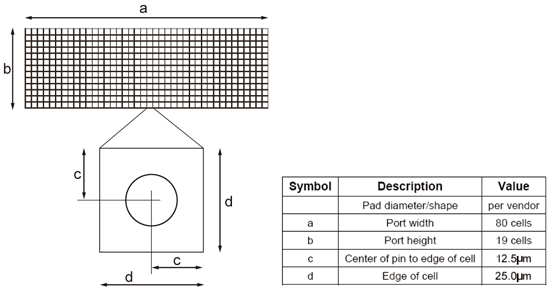 |
《表四 IMIS 標準之Pin Port定義(Columns Through 9) 》  Pin Port 說明:這裡原有的標準可能有誤。因為,根據標準,高度只有450um,而每一個Cell為25um×25um,若是安排 19pin則需要475um。 |
(本文作者為工研院系統晶片科技中心主任室特別助理)
<參考資料:
[1].Philip Pieters, EUROPEAN MICROSYSTEM \& MICRO-NANO TECHNOLOGY NETWORK, IMEC, Available At: http://www.eminent-microtechnology.net/downloads/2-1_Deliverable.pdf, 2002
[2].Gilles Poupon, Integration and packaging components: new challenge for the System Integration, ESCT 2006 – WLP Panel Session, Available At: http://141.30.122.65/PanelDisc/3-Poupon-ESTC_Panel-Session.pdf, 2006
[3].張鼎張、鄭晃忠,楊正杰,銅金屬化製程簡介,National Nano Device Laboratories (NDL) 第五卷第三期,Available At: http://www.ndl.org.tw/cht/ndlcomm/P5_3/P5_3.htm, 2009
[4].Microsystems Packaging Research Center, College of Engineering, Georgia Tech. 3D All Silicon System Module (3DASSM) Consortium Workshop, Available At: http://www.prc.gatech.edu/events/3dassm, 2008
[5].Semiconductor International , 3D All Silicon System Module, Available At: http://www.semiconductor.net/event/2140152091.html, May.11, 2008
[6].3D IC Alliance, IMIS-Intimate Memory Interface Specification, Available At: http://3d-ic.org/standards.html , 2008
[7].Philip Garrou, Recent 3D IC Integration Activity, Semiconducgtor International, Available At: http://www.semiconductor.net/blog/200000420/post/490030649.html, Jul. 27, 2008
[8].Philip Garrou, 3D Equipment & Materials Vendors Consortium, Semiconducgtor International, Available At: http://www.semiconductor.net/blog/200000420/post/460013646.html?q=TSV, Aug. 26, 2007>
